01
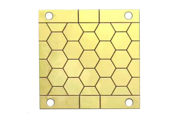
Alumina (Al2O3) PCB
96% - 99% Alumina content
Thermal conductivity: 24-30 W/m·K
Excellent dielectric properties
Superior thermal management with Alumina (Al2O3) and Aluminum Nitride (AlN) substrates for high-power, high-frequency, and aerospace applications.
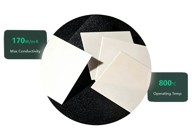
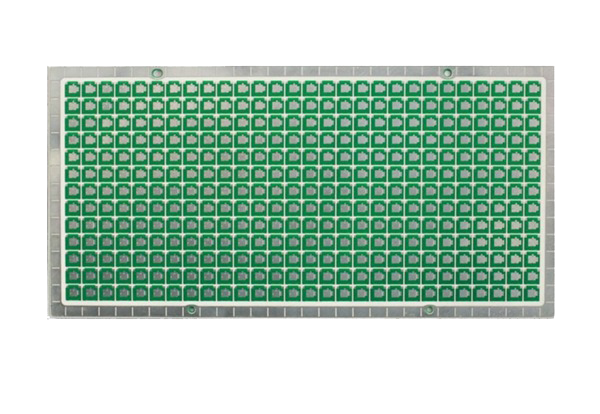
96% - 99% Alumina content
Thermal conductivity: 24-30 W/m·K
Excellent dielectric properties
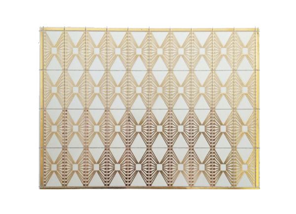
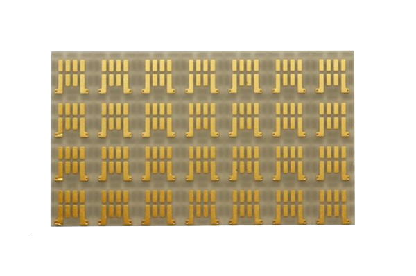
| Property | FR-4Standard/High TG | AluminumMetal Core | RogersHigh Frequency | CeramicAlumina/AlN |
|---|---|---|---|---|
| Thermal Conductivity | 0.25 W/m·K | 24 – 30 W/m·K | 150 – 170 W/m·K | 200+ W/m·K |
| Dielectric Constant | 4.2 – 4.6 | 9.0 - 10.0 | 8.5 - 9.0 | ~40 |
| Operating Temp | Up to 170°C | Up to 800°C | Up to 800°C | Up to 1000°C |
| CTE (Z-axis) | 50-70 ppm | 6-8 ppm | 4-5 ppm | 3.7 ppm |
| Durability | ||||
| Cost Level | ||||
| Best For | General purpose electronics | High-power LEDs, Automotive | RF, 5G, Radar Systems | Aerospace, High-power modules |

Selection of high-purity Alumina or Aluminum Nitride. Substrates undergo ultrasonic cleaning and surface treatment to ensure bonding quality.

Using CO2 or UV lasers to drill high-precision through-holes and scribe individual boards with micron-level accuracy.

Thin-film deposition (DPC) or high-temperature bonding (DBC) to create robust copper layers on the ceramic surface.

Fine-line circuit imaging followed by electroplating and high-end surface finishes like ENIG or Electrolytic Gold.
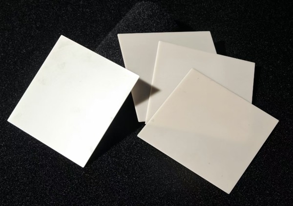
Seamlessly integrating flexible and rigid substrates to eliminate connectors, reduce weight, and maximize space in high-performance electronics.
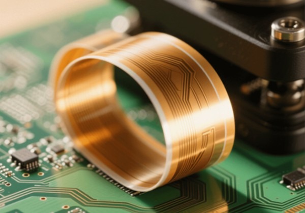
High-quality flexible and rigid-flex PCBs engineered for dynamic applications where space, weight and movement matter.

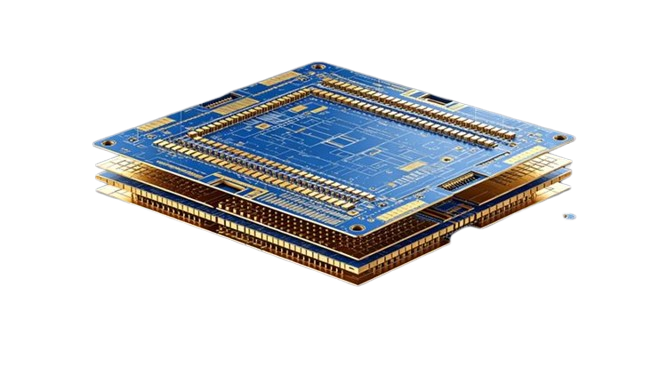
Leading-edge rigid PCB manufacturing services from single-sided to complex 56-layer multilayer boards with industry-leading precision.
Expert reverse engineering services to convert physical PCB samples into complete CAD files, Schematics, and BOM lists with guaranteed 100% precision.
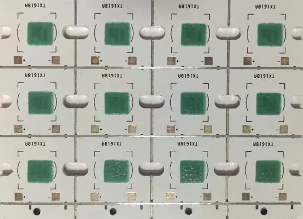
Material:Ceramic substrate;Layer:1L;
FinishBoardThickness:2.4mm;
MinLineWidth/Space:10/8mil;
MinHoleSize:0.6mm; SurfaceFinish:ENIG
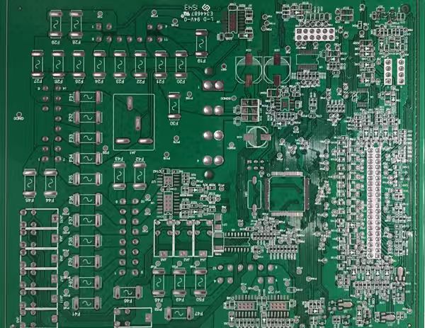
Material: FR‑4; Layers: 4L;
Finished board thickness: 1.6mm;
Trace width / trace spacing: 6/5mil;
Minimum hole size: 0.2mm;
Surface finish: OSP
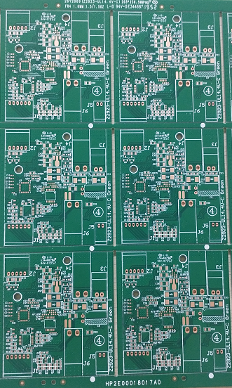
Material: FR‑4; Layers: 4L;
Finished board thickness: 2.0mm;
Trace width / trace spacing: 6/8mil;
Minimum hole size: 0.3mm;
Surface finish: Immersion Tin
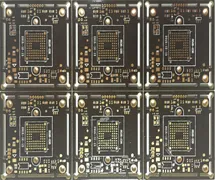
Material:FR-4 ;Layer:4L;
FinishBoardThickness:1.2mm;
MinLineWidth/Space:4/3mil;
MinHoleSize:0.15mm; SurfaceFinish:ENIG
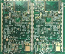
Material:FR-4 ;Layer:4L;
FinishBoardThickness:1.2mm;
MinLineWidth/Space:4/3mil;
MinHoleSize:0.15mm; SurfaceFinish:ENIG
Using the common ceramic circuit board thick film process, it is an advanced printed circuit board manufacturing technology with the advantages of easy multi-layer wiring, low cost, high temperature resistance, corrosion resistance, good mechanical strength, etc., which is widely used in the fields of electronics, communications, aerospace and so on.
According to the different needs, different processes, our factory can do ceramic circuit boards, can do the traditional process layer 2-8 layers, using low temperature co-fired ceramic (LTCC) and high temperature co-fired ceramic (HTCC), can reach 10-20 layers, or even higher. In actual application we will choose according to the customer, the type of process required and demand.
All of our products are IPC rated with ISO 14001; ISO 9001; CE; ROHS certificates, etc. Our products are widely used in communication, medical equipment, industrial control, power supply, consumer electronics and aerospace, automotive industry and other fields.
We can't produce without gerber file, we produce based on Gerber. Or if you have any samples, we can also clone based on the samples, if so, we can send 3-5 samples to our company, and then evaluate the price of making samples for you.
The fastest delivery time we can support is 12 hours. 1 hour for prompt quotation. 4 hours for prompt engineering. This depends on your product requirements and quantity. In addition, lead time will be included in your quote.