01
Multilayer PCB Cloning
Advanced techniques to clone complex 4-32 layer boards, including HDI structures and blind/buried vias.
- Layer-by-layer scanning
- Precise via mapping
- High-density interconnects
Expert reverse engineering services to convert physical PCB samples into complete CAD files, Schematics, and BOM lists with guaranteed 100% precision.
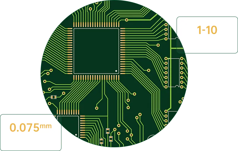
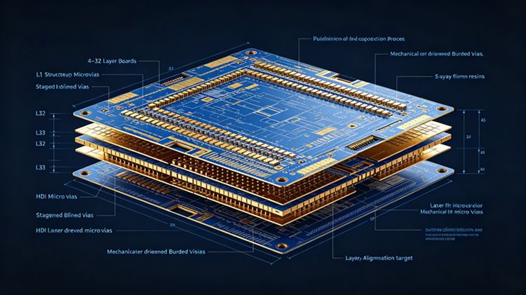
Advanced techniques to clone complex 4-32 layer boards, including HDI structures and blind/buried vias.
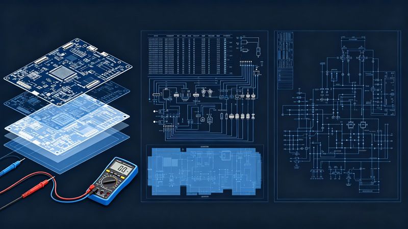
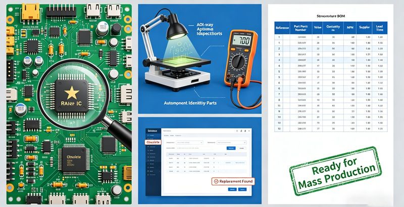
Full component identification including hard-to-find parts, providing a complete bill of materials for mass production.
Factor | Pure Cloning | Cloning + Mod | Optimization |
Functionality | Identical to Original | Modified/Improved | Enhanced Performance |
Time to Market | Fastest | Moderate | Balanced |
BOM Cost | Original Cost | Lowered | Optimized Cost |
Legacy Support | Perfect for Obsolescence | Upgraded Tech | Future Proofed |

Manufacturing a prototype from the new files to verify 100% functional equivalence with the original.


Detailed inspection of the physical sample and creation of the preliminary BOM list (Bill of Materials).

Seamlessly integrating flexible and rigid substrates to eliminate connectors, reduce weight, and maximize space in high-performance electronics.
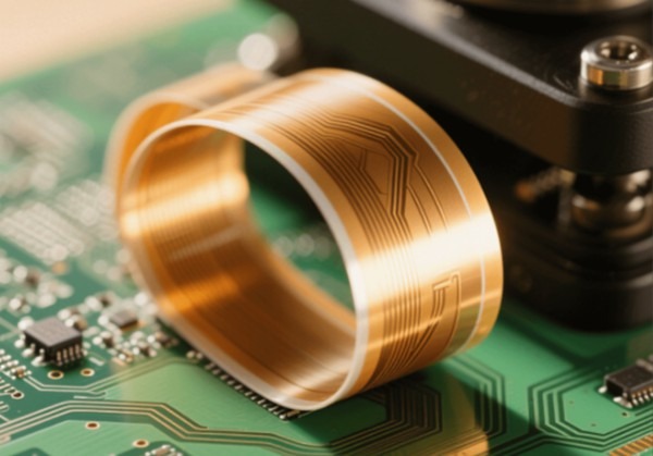
High-quality flexible and rigid-flex PCBs engineered for dynamic applications where space, weight and movement matter.
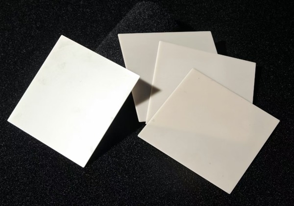
Superior thermal management with Alumina (Al2O3) and Aluminum Nitride (AlN) substrates for high-power, high-frequency, and aerospace applications.
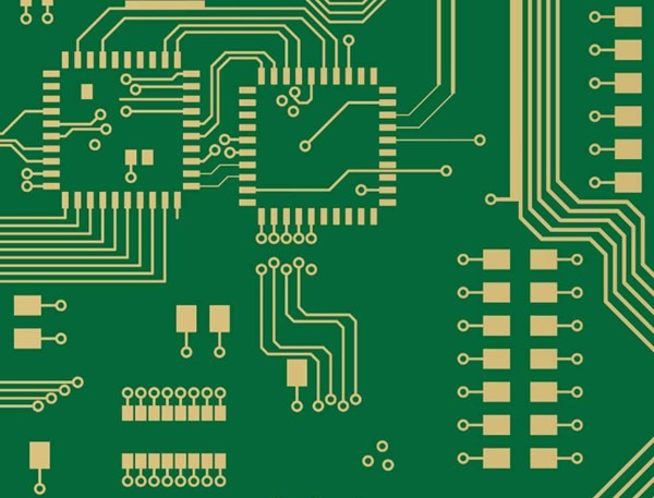
Leading-edge rigid PCB manufacturing services from single-sided to complex 56-layer multilayer boards with industry-leading precision.
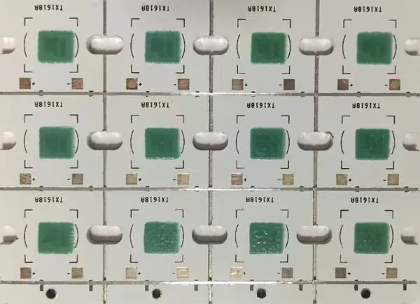
Material:Ceramic substrate;Layer:1L;
FinishBoardThickness:2.4mm;
MinLineWidth/Space:10/8mil;
MinHoleSize:0.6mm; SurfaceFinish:ENIG
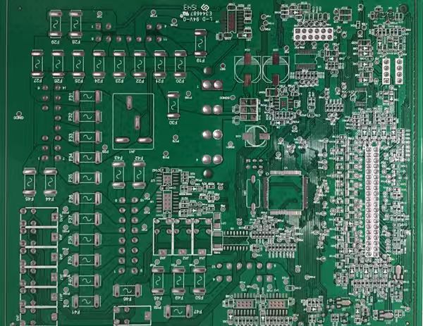
Material: FR‑4; Layers: 4L;
Finished board thickness: 1.6mm;
Trace width / trace spacing: 6/5mil;
Minimum hole size: 0.2mm;
Surface finish: OSP
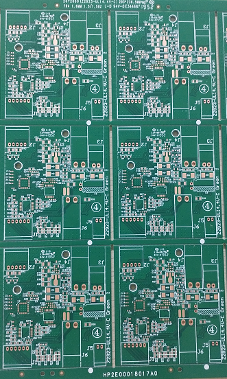
Material: FR‑4; Layers: 4L;
Finished board thickness: 2.0mm;
Trace width / trace spacing: 6/8mil;
Minimum hole size: 0.3mm;
Surface finish: Immersion Tin
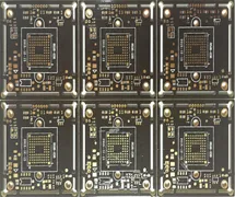
Material:FR-4 ;Layer:4L;
FinishBoardThickness:1.2mm;
MinLineWidth/Space:4/3mil;
MinHoleSize:0.15mm; SurfaceFinish:ENIG
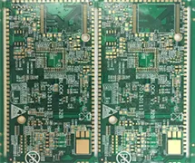
Material:FR-4 ;Layer:4L;
FinishBoardThickness:1.2mm;
MinLineWidth/Space:4/3mil;
MinHoleSize:0.15mm; SurfaceFinish:ENIG
Depending on the board complexity, PCB cloning can recover: PCB layout and Gerber files Schematic diagrams Bill of materials (BOM) Stack-up and layer information Key component footprints
PCB cloning is the process of reverse engineering an existing PCB to recreate its design data, including PCB layout, schematics, Gerber files, and bill of materials (BOM), so the board can be reproduced or manufactured again.