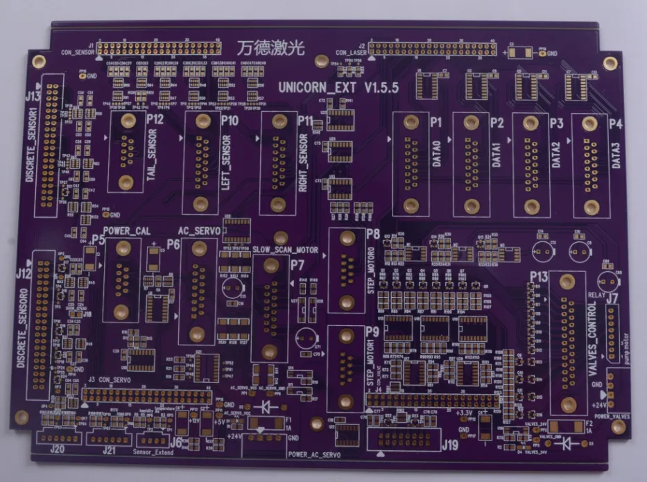


16-layer printed circuit boards (PCBs) have become a key technology carrier for complex system integration. Their design and manufacture involve precise interlayer control and signal integrity management. These multilayer boards perfectly balance high-density wiring requirements and signal integrity requirements through a precise laminated structure.
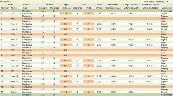
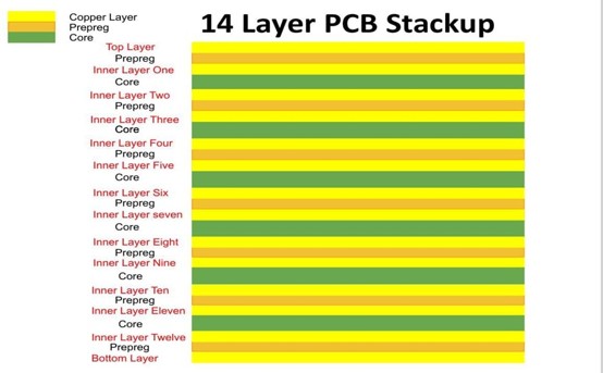
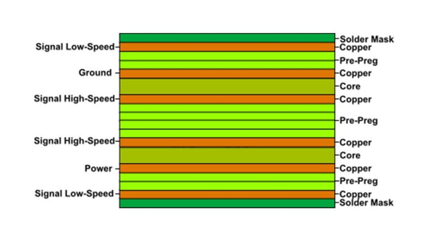
Typical laminate structure of a 16-layer PCB board
Configuration 1: High-Speed Signal Optimized (8S4P4G)
L1: Signal(TOP) L2: GND L3: Signal L4: Signal
L5: PWR1 L6: GND L7: Signal L8: Signal
L9: PWR2 L10:GND L11:Signal L12:Signal
L13:PWR3 L14:GND L15:Signal L16:GND(BOT)
Advantages:
Configuration 2: Mixed-Signal Processing Type
L1: RF Signal L2: GND L3: Analog L4: PWR
L5: Digital L6: GND L7: Digital L8: PWR
L9: Digital L10:GND L11:Digital L12:PWR
L13:Analog L14:GND L15:RF L16:GND
Features:
Configuration 3: High-Power Application Type
(Includes 2oz thick copper power layers and dedicated thermal layers)
Key Points:
Expert Recommendation: Conduct 3D electromagnetic field simulations when selecting stackup configurations. Ansys HFSS or CST Studio Suite are recommended for design validation.
16-layer PCB design and manufacturing
Critical Material Technology and Thickness Control
1. High-End Material Selection
Material Type | Typical Model | Dk@10GHz | Df@10GHz | Applications |
High-Speed FR4 | Megtron6 | 3.7 | 0.002 | 112G SerDes |
Low-Loss Material | RO4835 | 3.5 | 0.003 | mmWave Radar |
High-Tg Material | IT-180A | 4.3 | 0.012 | Automotive Electronics |
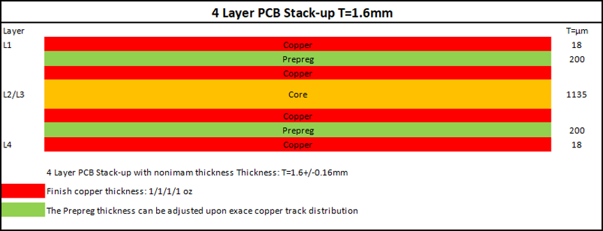
2. Thickness Control System
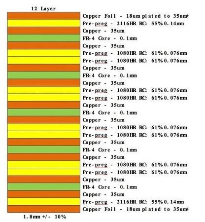
Example for 1.6mm board thickness:
Calculation Formula:
Total Thickness = Σ(Copper thickness) + Σ(Dielectric thickness) + Solder mask thickness
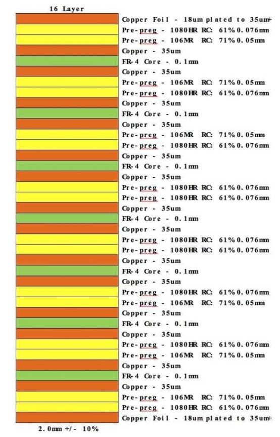
Advanced Manufacturing Process Flow
Quality Inspection Standards:
Signal Integrity Design
Case Study: A 5G base station AAU using 16-layer PCBs achieved 32% lower insertion loss, 28% better thermal performance, and 100,000 hours MTBF reliability.
Recommended Professional Manufacturing Services
TUOGEE offers premium 16-layer PCB turnkey solutions:
✅ Up to 32-layer custom stackup
✅ ±5% impedance control
✅ 100μm laser blind vias
✅ 3D printed rapid prototypes
✅ Complete SI/PI simulation services
FQA Highlights
Q: How to balance cost and performance in 16-layer designs?
A: Recommended “4+8+4” hybrid lamination: 4 high-speed material layers + 8 FR4 layers reduces cost by 15% while maintaining critical signal layer performance.
Q: How to address thermal challenges in 16-layer boards?
A: Three effective solutions:
Q: Common defects in 16-layer board mass production?
A: Key focus areas:
Applications of 16-Layer PCBs
16-layer printed circuit boards perfectly balance high-density routing needs with signal integrity requirements through precise stackup structures, finding widespread applications in:
Typical Technical Parameters: